 40G/100G Optical Transceivers
 25G Optical Transceivers
 10G Optical Transceivers
 155M/2.5G Optical Transceivers
 1G Optical Transceivers
 FC 16G/32G Optical Transceivers
 1G BIDI Optical Transceivers
 Dual-Rate Optical Transceivers
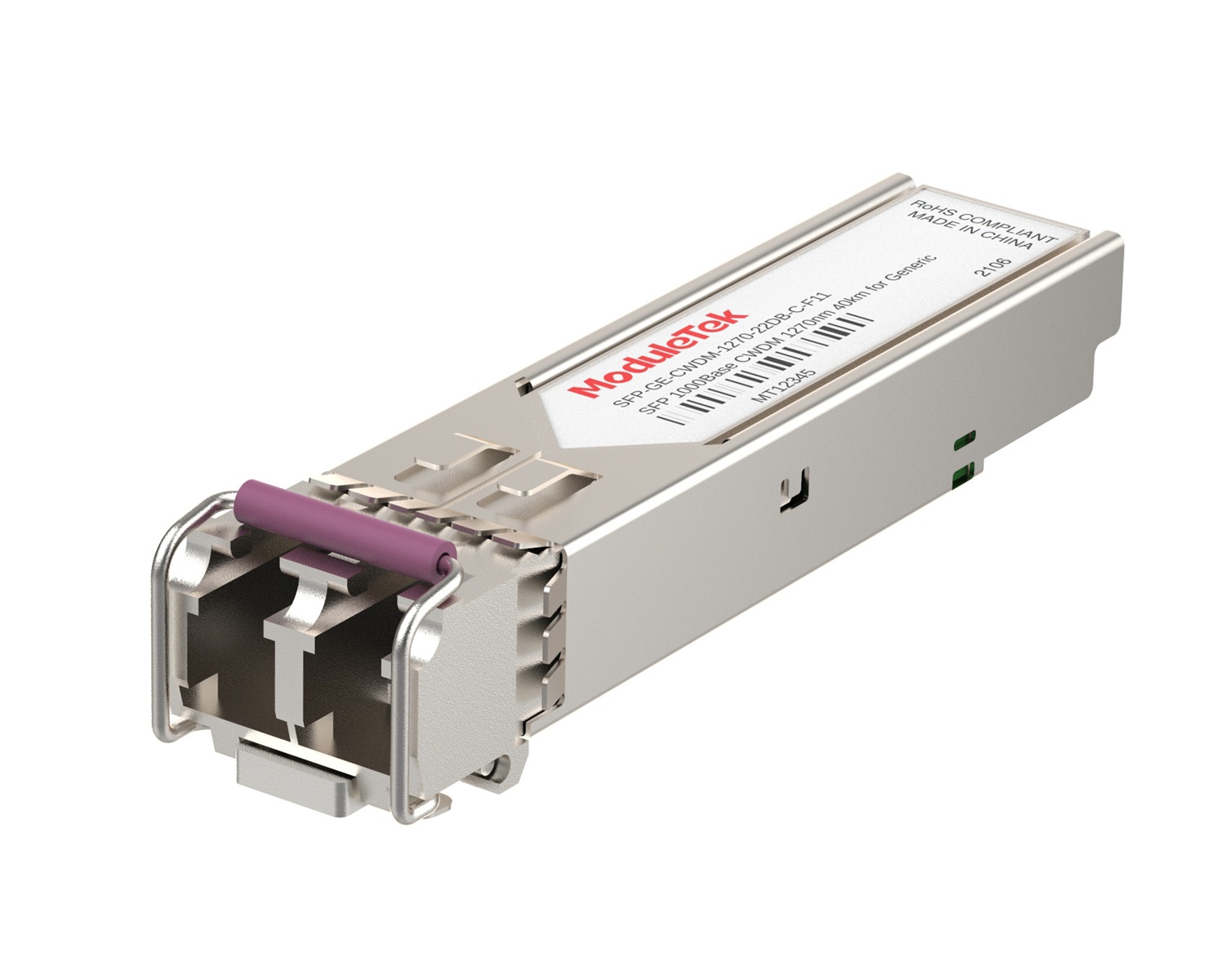 CWDM Optical Transceivers
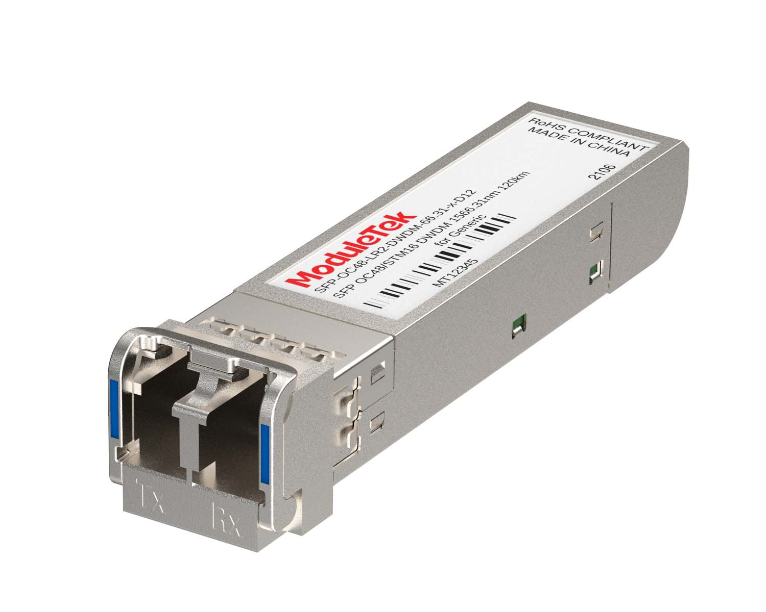 DWDM Optical Transceivers
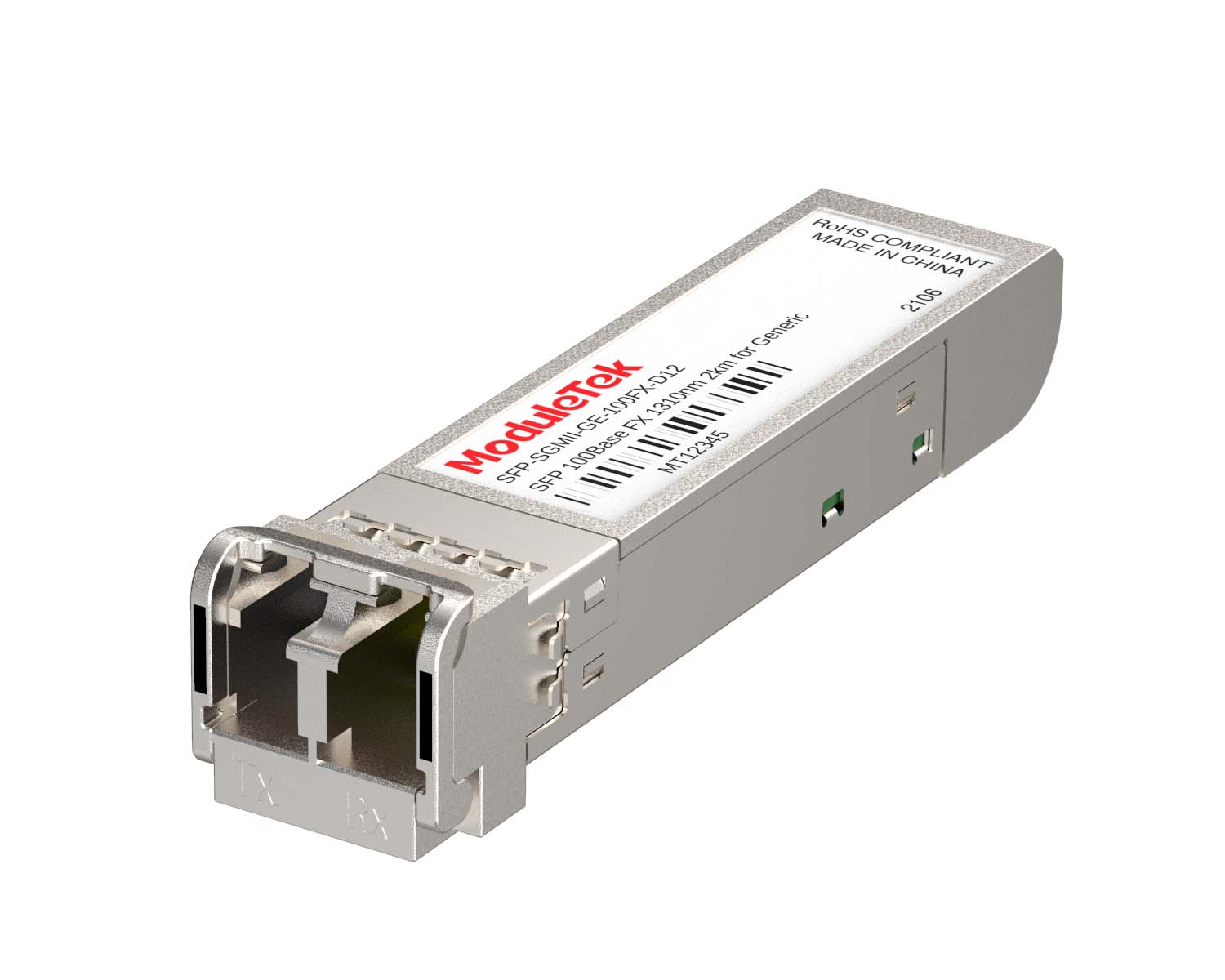 SGMII Port Optical Transceivers
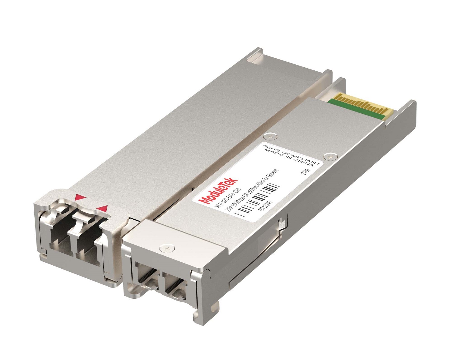 XFP Optical Transceivers
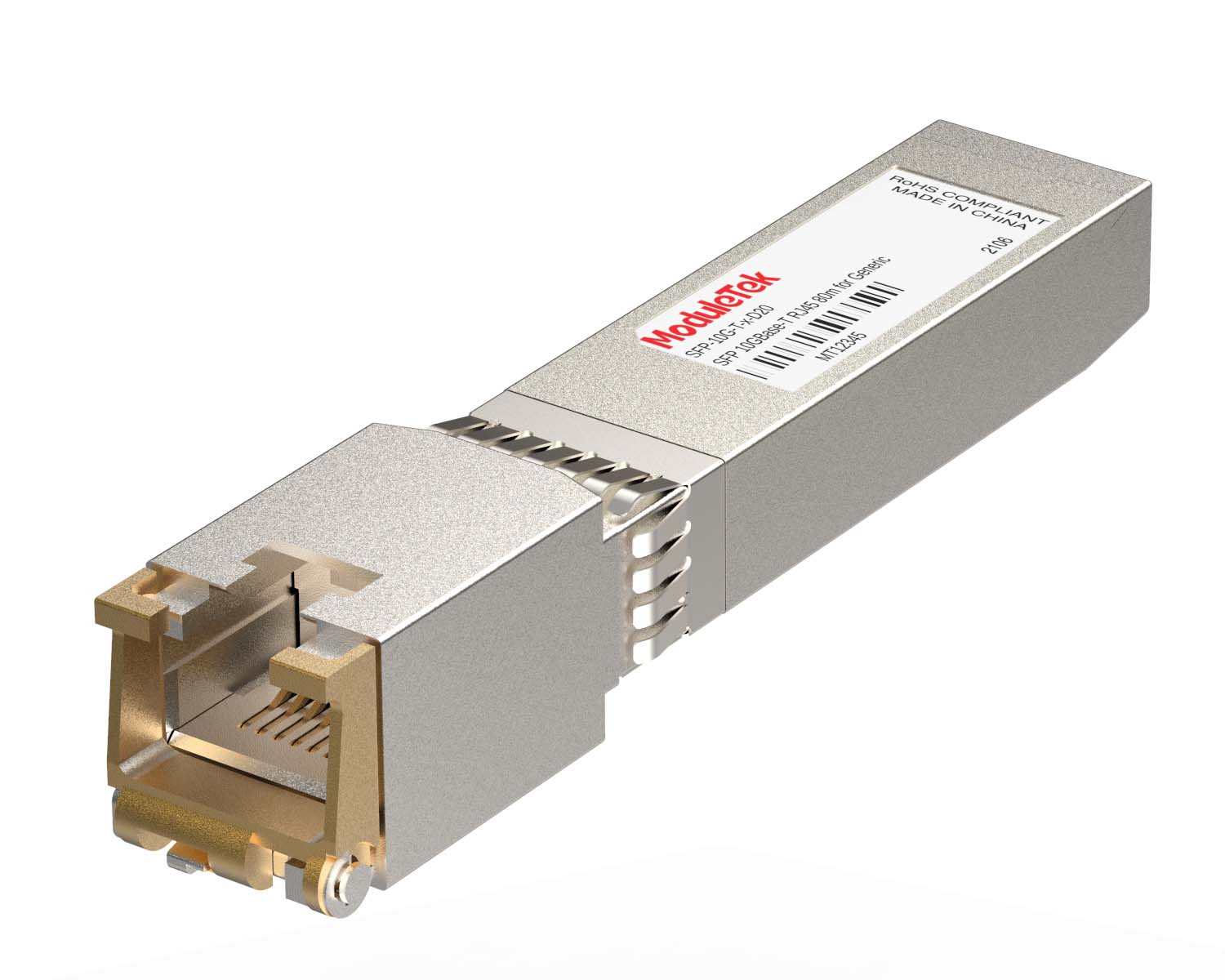 100M/1G/10G Coppers
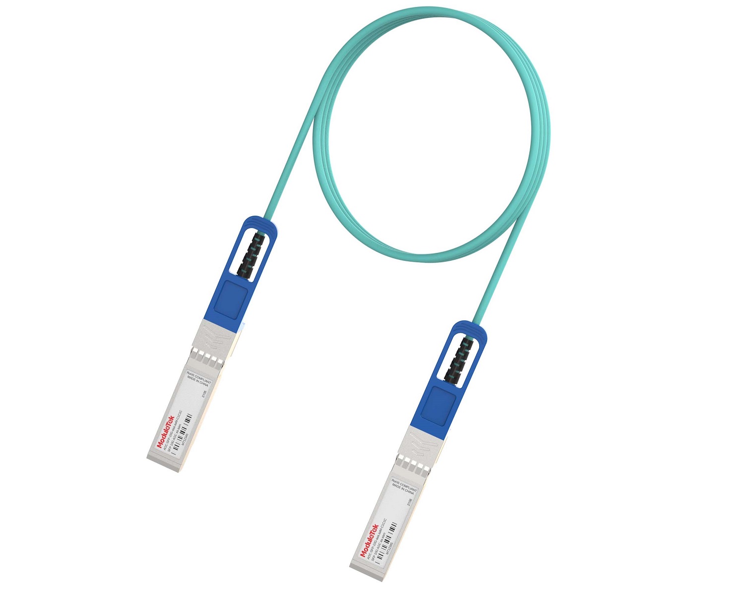 Full-Rate AOC & Breakout Series
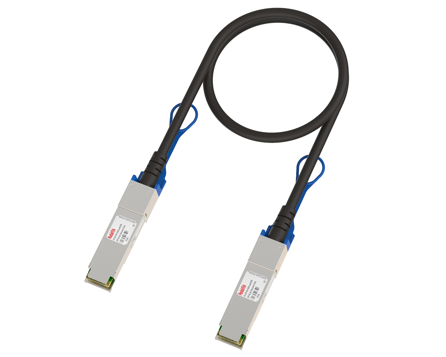 10G/40G Active DAC Series
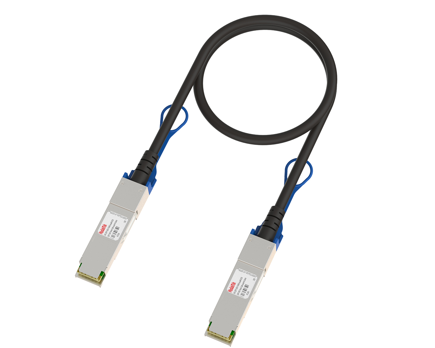 Full-Rate Passive DAC Series
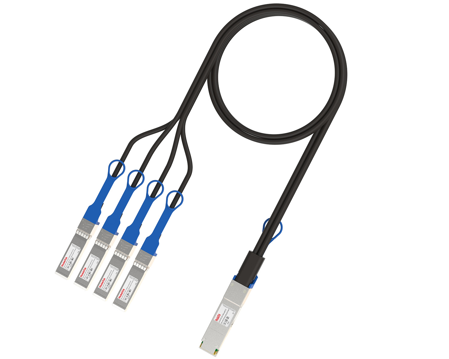 40G/100G Passive Breakout DAC Series
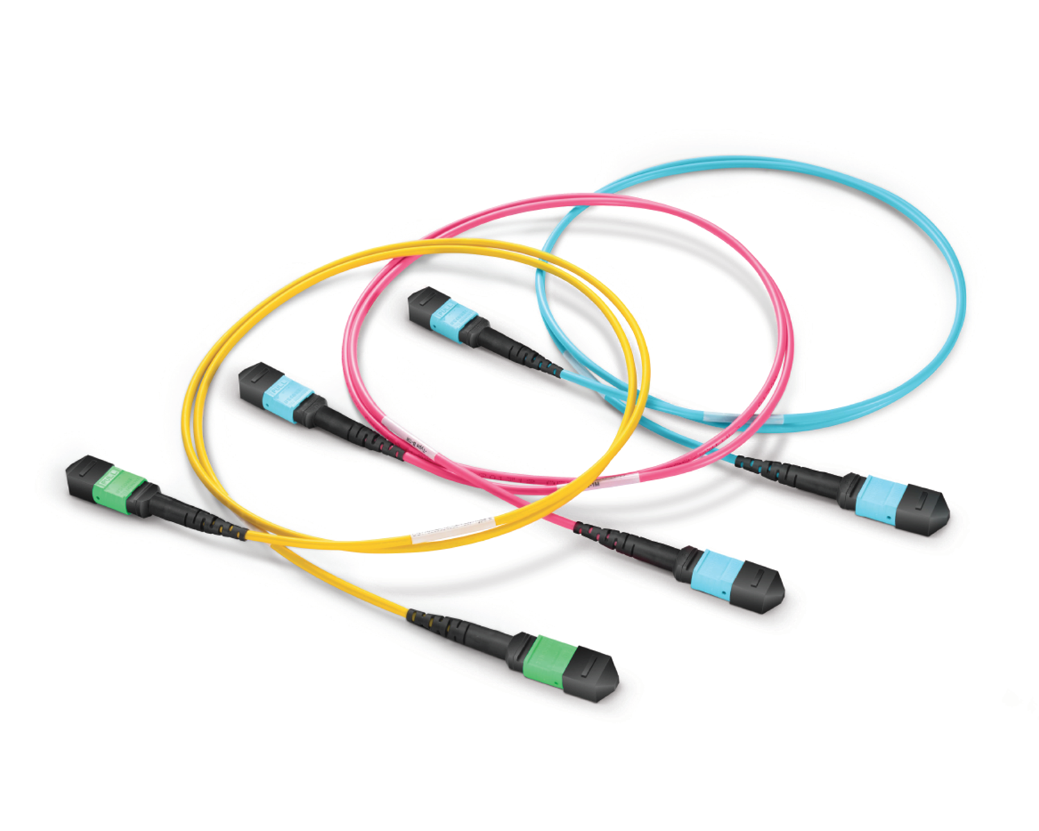 Regular/MTP-MPO Fiber Patch Cords
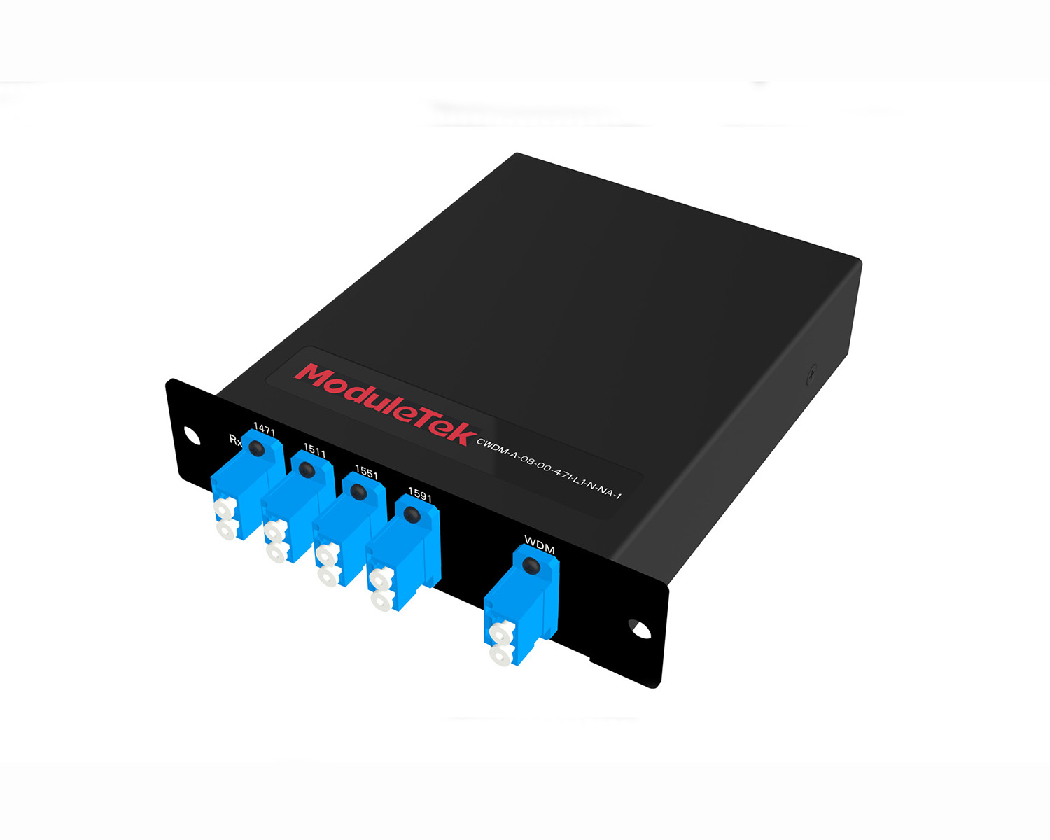 MT2011
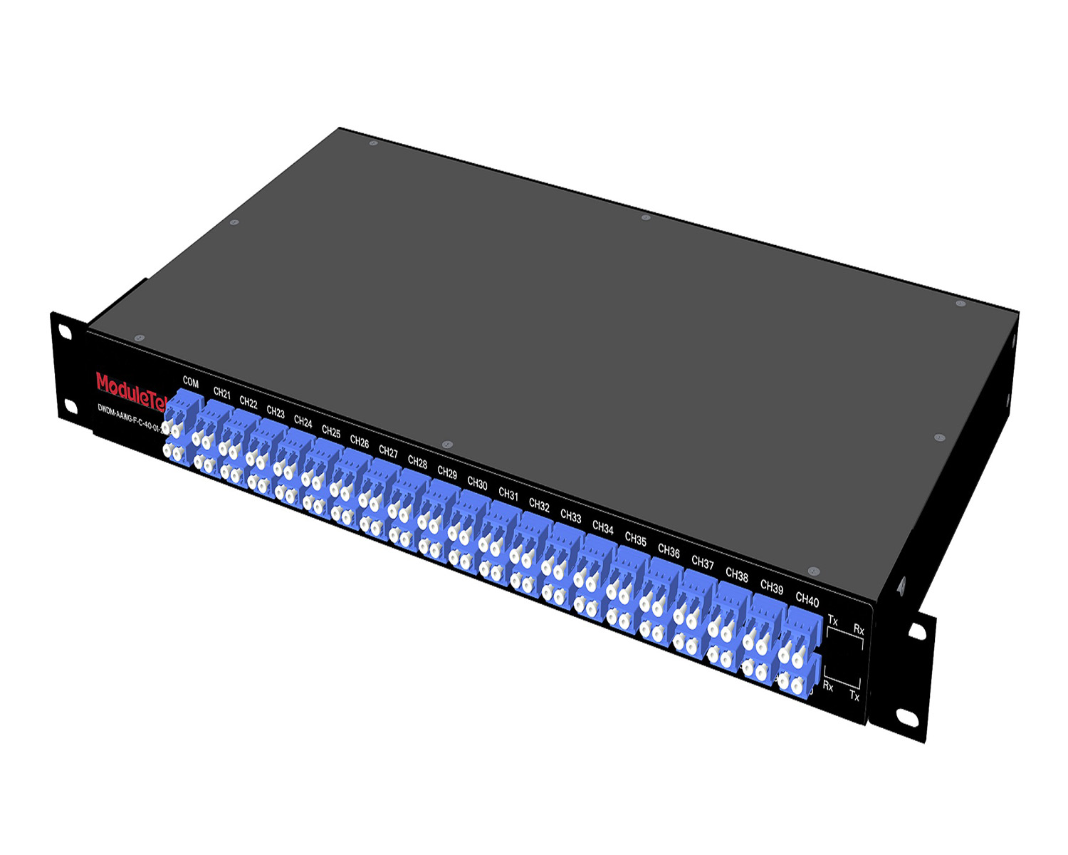 MT2010
 CodingBox
 QSFP to SFP Adapter
Introduction To The COB Process For Optical Modules
Time: 2020-02-20
1. What is the COB Process?
In recent years, the COB (Chip-on-Board) process has been frequently mentioned in the context of high-speed optical modules. The COB process refers to a technology that directly mounts bare chips onto a printed circuit board (PCB), connects them via gold wire bonding, and then encapsulates and protects the chips and wires using organic adhesive. Compared with conventional processes, the COB process offers high packaging density, simplified procedures, minimal signal integrity issues, and a certain cost advantage.
2. Main Procedures of the COB Process
The COB process mainly consists of three key steps: die bonding, wire bonding, and optical coupling.
2.1 Die Bonding
Bare chips are attached to the surface of a PCB using conductive silver adhesive with high-precision die bonding equipment, as illustrated in the diagram below. The process flow is as follows: first, the equipment identifies the designated die bonding positions on the PCB. A dispensing needle then applies an appropriate amount of silver adhesive to these positions. Next, the machine nozzle picks up optical chips and electrical chips from the material tray and places them respectively on the adhesive-coated areas. After manual inspection of the die bonding accuracy, the chips are permanently secured through high-temperature baking.
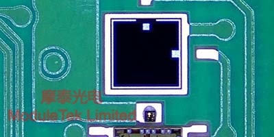
Figure 1: Die Bonding Schematic Diagram
2.2 Wire Bonding
Wire bonding involves bonding gold wires between electrical chips and optical chips, as well as between electrical chips and PCB pads, to achieve both electrical and mechanical connections. This step is typically completed using a wire bonder. Both die bonding and wire bonding are critical processes. The bonded wires must pass tensile strength tests, and strict requirements are imposed on wire length—both excessively long and short wires can affect actual performance parameters such as sensitivity and transmit eye diagram quality. In fact, wire bonding defects are a common root cause identified in optical module failure analysis.
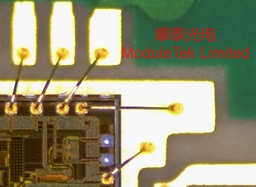
Figure 2: Wire Bonding Schematic Diagram
2.3 Optical Coupling
Optical coupling refers to the process of mounting a precision lens onto the PCB to reflect the vertically emitted light from the VCSEL (Vertical-Cavity Surface-Emitting Laser) into a parallel beam. This step is crucial to module performance: a misaligned lens or improper application of UV adhesive can lead to variations and inconsistencies in output optical power and receiver sensitivity.
The general operational process is as follows: after loading the program into the PCB substrate that has undergone die bonding and wire bonding, an automatic coupling machine adjusts the adapter lens to an optimal position for maximizing light transmission and reception efficiency. The lens is first temporarily fixed with UV adhesive, followed by permanent curing with black adhesive, which is finalized through several hours of high-temperature baking. The COB automatic coupling machine enables high levels of automation, requiring only manual loading and unloading of materials. It can perform automatic coupling and dispensing, significantly improving the overall module manufacturing efficiency.
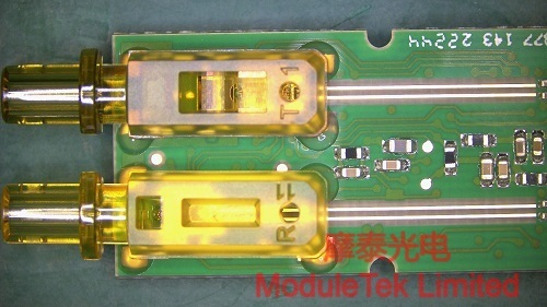
Figure 3: Optical Coupling Diagram
Moduletek operates its own die bonding, wire bonding, and automatic coupling production lines, and can supply a wide range of optical module products manufactured with the COB process. Welcome to contact us for inquiries and purchases.
If you have any questions about the above content, please contact us via email: sales@moduletek.com


